Nanometer scale characterization of a GaAsP semiconductor
August 23, 2022
 Download This Application
Introduction
The NFS Series of scanning near-field optical microspectrometers have been optimized as a new solution for nanotechnology applications. Traditionally, characterization methods on the nanometer scale consist of topography observation using an electron or scanning probe microscope or elemental analysis using an x-ray microanalyzer. These methods deliver images with high spatial resolution but they cannot obtain chemical information from a sample surface. On the other hand, traditional FT-IR, photoluminescence, or Raman microspectroscopy instruments can provide chemical data for a sample, but the spatial resolution is determined by the diffraction limit of light, limited to the wavelength of the light used. Scanning near-field microspectrometers allow characterization at the extreme nano level range exceeding the diffraction limit of light. Introducing light into a fiber probe with an aperture of a hundred to several hundred nm produces near-field light of the same size as the probe aperture. Bringing the sample close to the probe aperture (within 100 nm) allows spectroscopic observations with a spatial resolution of several hundred nm as a result of the interaction of the near-field light with the sample surface.
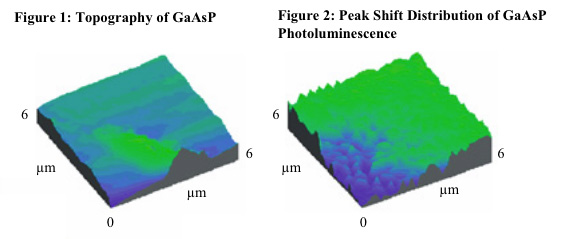
Sample characterization with submicron spatial resolution is critical because impurities on the nanometer scale can have a major impact on the electrical properties of semiconductors. For instance, the compositional ratio of GaAs and GaP in a GaAsP material can be estimated from the emission spectra of the sample surface. Conventional nearfield microscopes that do not provide spectroscopic data cannot produce this compositional information. With the NFS series, however, observation of minute peak shifts from the emission spectra can easily be performed for multiple sample sites. Figure 1 is the topographical image of a sample surface for a 6 x 6 µm area. Figure 2 illustrates the peak shift distribution of the GaAsP substrate, the green portions denoting a long wavelength shift, indicating that the GaP concentration is slightly higher than the surrounding area.
Featured Products:
-
SFC-4000 Preparative, Semi-Preparative, and Hybrid SFC systems for preparative scale purifications.
Preparative SFC
-
LC-4000 Series Preparative HPLC
-
SFC-4000 Semi-Preparative SFC for semi-preparative scale purifications.
Semi-Preparative SFC System

Nanometer scale characterization of a GaAsP semiconductor
Introduction
The NFS Series of scanning near-field optical microspectrometers have been optimized as a new solution for nanotechnology applications. Traditionally, characterization methods on the nanometer scale consist of topography observation using an electron or scanning probe microscope or elemental analysis using an x-ray microanalyzer. These methods deliver images with high spatial resolution but they cannot obtain chemical information from a sample surface. On the other hand, traditional FT-IR, photoluminescence, or Raman microspectroscopy instruments can provide chemical data for a sample, but the spatial resolution is determined by the diffraction limit of light, limited to the wavelength of the light used. Scanning near-field microspectrometers allow characterization at the extreme nano level range exceeding the diffraction limit of light. Introducing light into a fiber probe with an aperture of a hundred to several hundred nm produces near-field light of the same size as the probe aperture. Bringing the sample close to the probe aperture (within 100 nm) allows spectroscopic observations with a spatial resolution of several hundred nm as a result of the interaction of the near-field light with the sample surface.
Sample characterization with submicron spatial resolution is critical because impurities on the nanometer scale can have a major impact on the electrical properties of semiconductors. For instance, the compositional ratio of GaAs and GaP in a GaAsP material can be estimated from the emission spectra of the sample surface. Conventional nearfield microscopes that do not provide spectroscopic data cannot produce this compositional information. With the NFS series, however, observation of minute peak shifts from the emission spectra can easily be performed for multiple sample sites. Figure 1 is the topographical image of a sample surface for a 6 x 6 µm area. Figure 2 illustrates the peak shift distribution of the GaAsP substrate, the green portions denoting a long wavelength shift, indicating that the GaP concentration is slightly higher than the surrounding area.