Automated Measurement of the Film Thickness of Epitaxial Layers on Semi-Conductor Wafers using IR or NIR Analysis
June 13, 2024
 Download This Application
Introduction
The thickness of epitaxial layers, substrate, etching (residual layer), liquid crystal cell gap, and other semiconductor layers dramatically impacts semiconductor device performance. Management of layer thickness during the manufacturing process is extremely crucial for the production of large yields of stable devices.
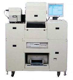
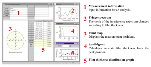
The UTS-200 epitaxial layer thickness measurement system is an automated non-destructive, non-contact analysis method using the latest interferometric technology to provide rapid film thickness measurements. Utilizing a proprietary frequency analysis method, the sample interference spectrum is converted into a spatialgram and the thickness of the layer is calculated with a high degree of accuracy. This integrated system offers the film thickness measurements required for the exacting standards of the semiconductor industry, including: high-speed sample mapping, a wide measurement range; and a refined operating environment, supporting a wide range of analysis requirements from process use to R&D. JASCO offers near-infrared and mid-infrared models according to the thickness measurements desired.
Featured Products:
-
Film Holders for UV-Visible/NIR Spectrophotometers
-
UV-Visible/NIR Spectra Manager™
-
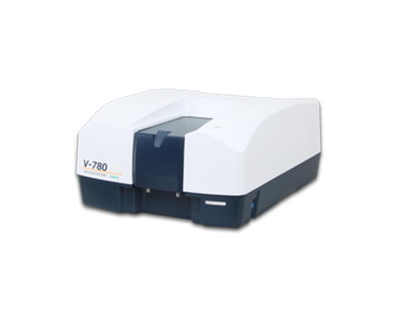
A high sensitivity UV-Visible/NIR Spectrophotometer with InGaAs detector for wavelengths up to1600nm
V-780 UV-Visible/NIR Spectrophotometer

Automated Measurement of the Film Thickness of Epitaxial Layers on Semi-Conductor Wafers using IR or NIR Analysis
Introduction
The thickness of epitaxial layers, substrate, etching (residual layer), liquid crystal cell gap, and other semiconductor layers dramatically impacts semiconductor device performance. Management of layer thickness during the manufacturing process is extremely crucial for the production of large yields of stable devices.
The UTS-200 epitaxial layer thickness measurement system is an automated non-destructive, non-contact analysis method using the latest interferometric technology to provide rapid film thickness measurements. Utilizing a proprietary frequency analysis method, the sample interference spectrum is converted into a spatialgram and the thickness of the layer is calculated with a high degree of accuracy. This integrated system offers the film thickness measurements required for the exacting standards of the semiconductor industry, including: high-speed sample mapping, a wide measurement range; and a refined operating environment, supporting a wide range of analysis requirements from process use to R&D. JASCO offers near-infrared and mid-infrared models according to the thickness measurements desired.