Thickness distribution of thin films by ellipsometry
May 4, 2017
Introduction
The M-500 is a Spectroscopic Ellipsometer with Photo Elastic Modulator (PEM) optics and a patented optical servo for reference control. The M-500 is specifically designed for use in a semiconductor clean room or fabrication facility, using a horizontal sample introduction system. Coupled with a robotic wafer handling system, high throughput automated measurements are easily conducted. An automatic sample stage with a sample mapping program can measure the thickness distribution of thin films on a wafer. The integrated software includes various options such as multi-layer analysis, wavelength dispersion measurements of optical constants and other optional analysis programs.
Diagram of PEM Principle

Mapping measurement
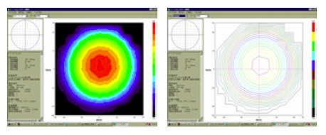
The mapping measurement takes advantage of the PEM system’s high speed to enable film thickness and refractivity distribution measurement within a maximum of an 8 inch diameter of the sample surface. The mapping measurement program offers display features including 3-D representation, contour map, and color map. The figure shows the thickness distribution of silicon oxide on a four-inch substrate. An average film thickness and average refractive index of 902A and 2.01, respectively, is obtained. The film is thicker towards the center and thinner towards the edge of the wafer.


Thickness distribution of thin films by ellipsometry
Introduction
The M-500 is a Spectroscopic Ellipsometer with Photo Elastic Modulator (PEM) optics and a patented optical servo for reference control. The M-500 is specifically designed for use in a semiconductor clean room or fabrication facility, using a horizontal sample introduction system. Coupled with a robotic wafer handling system, high throughput automated measurements are easily conducted. An automatic sample stage with a sample mapping program can measure the thickness distribution of thin films on a wafer. The integrated software includes various options such as multi-layer analysis, wavelength dispersion measurements of optical constants and other optional analysis programs.
Diagram of PEM Principle

Mapping measurement
The mapping measurement takes advantage of the PEM system’s high speed to enable film thickness and refractivity distribution measurement within a maximum of an 8 inch diameter of the sample surface. The mapping measurement program offers display features including 3-D representation, contour map, and color map. The figure shows the thickness distribution of silicon oxide on a four-inch substrate. An average film thickness and average refractive index of 902A and 2.01, respectively, is obtained. The film is thicker towards the center and thinner towards the edge of the wafer.


 Download This Application