Evaluation of a Luminescent Semiconductor on the Nanometer Scale
August 23, 2022
 Download This Application
Introduction
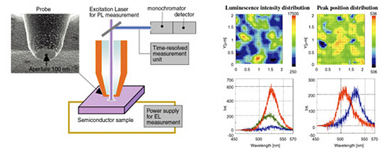
Photoluminescence (PL) and electroluminescence (EL) measurements are standard techniques for evaluation of the crystallinity, functionality and luminescent mechanism of semiconductors. For these samples, near-field optical microscopy is the only effective method for characterization of the composition and distribution of luminescent centers on the nanometer scale.
In combination with a superconductive magnetic field, luminescent spectral measurements of the sample surface can be accomplished with nano-scale spatial resolution while applying temperatures as low as 7K and magnetic fields as high as 4 Tesla.
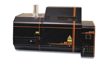
Luminescent Measurement of InGaN by NFS Series Scanning Near-Field Optical Microspectrometer
Featured Products:
-
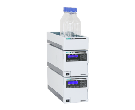
SFC-4000 Analytical SFC for routine separation to method development.
Analytical SFC System
-
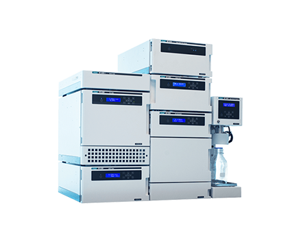
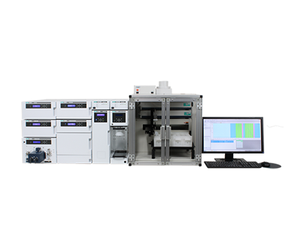
LC-4500 Series Compact HPLC
-
SFC-4000 Hybrid SFC for analytical and semi-preparative SFC.
Hybrid SFC System

Evaluation of a Luminescent Semiconductor on the Nanometer Scale
Introduction
Photoluminescence (PL) and electroluminescence (EL) measurements are standard techniques for evaluation of the crystallinity, functionality and luminescent mechanism of semiconductors. For these samples, near-field optical microscopy is the only effective method for characterization of the composition and distribution of luminescent centers on the nanometer scale.
In combination with a superconductive magnetic field, luminescent spectral measurements of the sample surface can be accomplished with nano-scale spatial resolution while applying temperatures as low as 7K and magnetic fields as high as 4 Tesla.
Luminescent Measurement of InGaN by NFS Series Scanning Near-Field Optical Microspectrometer