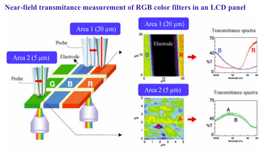
Transmittance Near-field measurements in the UV-visible/NIR range at 0.1 to 1 µm spatial resolution
August 23, 2022
Introduction
Photoluminescence (PL) and electroluminescence (EL) measurements are standard techniques for evaluation of the crystallinity, functionality and luminescent mechanism of semiconductors. For these samples, near-field optical microscopy is the only effective method for characterization of the composition and distribution of luminescent centers on the nanometer scale.
In combination with a superconductive magnetic field, luminescent spectral measurements of the sample surface can be accomplished with nano-scale spatial resolution while applying temperatures as low as 7K and magnetic fields as high as 4 Tesla.
Luminescent Measurement of InGaN by NFS Series Scanning Near-Field Optical Microspectrometer
Featured Products:
-
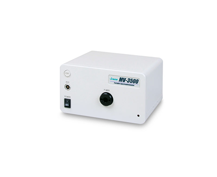
MV-3000 Series Portable UV-Visible/NIR Spectrophotometer
-
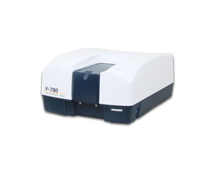
A high sensitivity UV-Visible/NIR Spectrophotometer with InGaAs detector for wavelengths up to1600nm
V-780 UV-Visible/NIR Spectrophotometer
-
Spectra Manager™ Spectroscopy Software

Transmittance Near-field measurements in the UV-visible/NIR range at 0.1 to 1 µm spatial resolution
Introduction

Photoluminescence (PL) and electroluminescence (EL) measurements are standard techniques for evaluation of the crystallinity, functionality and luminescent mechanism of semiconductors. For these samples, near-field optical microscopy is the only effective method for characterization of the composition and distribution of luminescent centers on the nanometer scale.
In combination with a superconductive magnetic field, luminescent spectral measurements of the sample surface can be accomplished with nano-scale spatial resolution while applying temperatures as low as 7K and magnetic fields as high as 4 Tesla.
Luminescent Measurement of InGaN by NFS Series Scanning Near-Field Optical Microspectrometer


 Download This Application