Measurement of the Transition Process of a Semiconductor
August 23, 2022
 Download This Application
Introduction
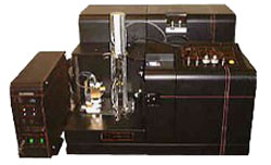
Emission or absorption time course measurements enable us to observe excitation electrons or energy dynamics and to understand how the place of observation or the environment influences the semiconductor transitions. Figure 1 illustrates the emission spectrum of a semiconductor substrate InP. Two peaks appear and they demonstrate the differences in the transition process from the excitation state to the ground state. Figure 2 demonstrates the data from a time resolved measurement of the two peaks. The attenuation time of the peak of the lower energy side (longer wavelength) was longer than that of the higher energy side (shorter wavelength). Most likely, the peak due to the lower wavelength was trapped by a donor receptor during the transition process.
Featured Products:
-
A powerful combination of performance, sensitivity and flexibility for biological, environmental and materials analysis.
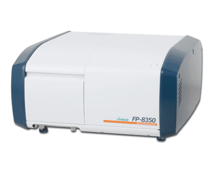
FP-8350 Spectrofluorometer
-
Uniquely optimized for NIR applications with extended wavelength measurement to 1010 nm.
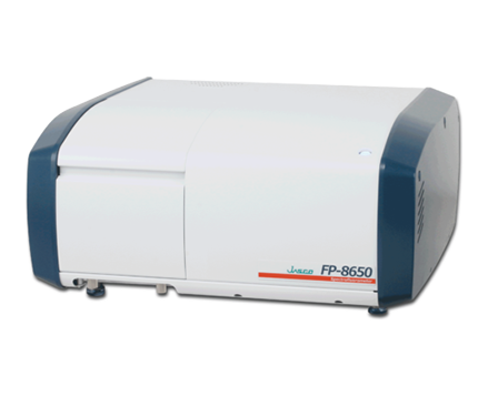
FP-8650 NIR Spectrofluorometer
-
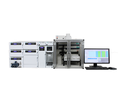
SFC-4000 Hybrid SFC for analytical and semi-preparative SFC.
Hybrid SFC System

Measurement of the Transition Process of a Semiconductor
Introduction
Emission or absorption time course measurements enable us to observe excitation electrons or energy dynamics and to understand how the place of observation or the environment influences the semiconductor transitions. Figure 1 illustrates the emission spectrum of a semiconductor substrate InP. Two peaks appear and they demonstrate the differences in the transition process from the excitation state to the ground state. Figure 2 demonstrates the data from a time resolved measurement of the two peaks. The attenuation time of the peak of the lower energy side (longer wavelength) was longer than that of the higher energy side (shorter wavelength). Most likely, the peak due to the lower wavelength was trapped by a donor receptor during the transition process.