Semiconductor Stress Measurement
August 24, 2022
 Download This Application
Introduction
Raman Spectrometers
<h3″>Stress evaluation of Silicon (Si)
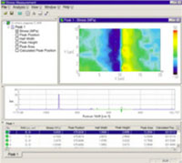
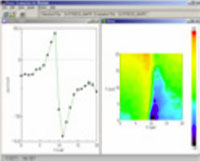
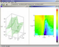
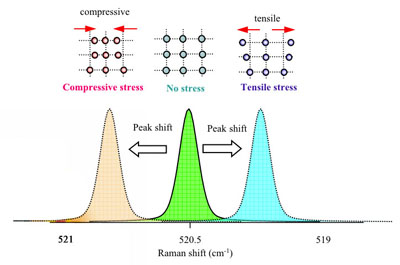
The evaluation of stress in silicon devices is extremely important in the development of next generation, high precision, highly integrated devices. Since the Raman spectrum reflects the degree of pressure dependence on the sample’s lattice vibration, it can detect stress in silicon and other semiconductors. The amount of stress is calculated from the Raman peak shift of Si. Stress-free Si has a sharp peak at around 520 cm-1. If compression stress is exerted on the crystal lattice, the lattice constant decreases and the coupling strength increases. Accordingly, the lattice vibration energy increases and the peak will shift towards higher wave numbers. When the compression is released, the peak will shift in the opposite direction to lower wavenumbers.
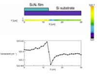
Stress distribution of a nitrided film
Featured Products:

Semiconductor Stress Measurement
Introduction
Raman Spectrometers
<h3″>Stress evaluation of Silicon (Si)
The evaluation of stress in silicon devices is extremely important in the development of next generation, high precision, highly integrated devices. Since the Raman spectrum reflects the degree of pressure dependence on the sample’s lattice vibration, it can detect stress in silicon and other semiconductors. The amount of stress is calculated from the Raman peak shift of Si. Stress-free Si has a sharp peak at around 520 cm-1. If compression stress is exerted on the crystal lattice, the lattice constant decreases and the coupling strength increases. Accordingly, the lattice vibration energy increases and the peak will shift towards higher wave numbers. When the compression is released, the peak will shift in the opposite direction to lower wavenumbers.
Stress distribution of a nitrided film